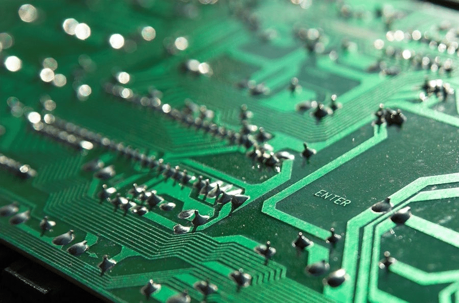
The increasing demand for high-performance electronic systems has created a growing need for printed circuit boards capable of handling substantial electrical currents, elevated temperatures, and demanding operating conditions. Traditional printed circuit boards are suitable for many electronic applications, but high-power systems often require specialized designs with improved current-carrying capacity and thermal management. This is where heavy copper pcb manufacturers play an essential role in modern electronics production.
Heavy copper printed circuit boards are engineered with thicker copper layers than conventional PCBs, allowing them to support higher electrical currents and improved heat distribution when properly designed. These specialized circuit boards are widely used in power electronics, industrial automation, automotive systems, renewable energy equipment, and other demanding applications.
FastTurn PCBA provides PCB manufacturing and assembly solutions for businesses developing advanced electronic products. For organizations exploring heavy copper PCB technology, understanding manufacturing requirements, design considerations, and quality standards is essential for selecting a suitable production partner.
Understanding Heavy Copper PCB Technology
Heavy copper PCBs are printed circuit boards manufactured with copper layers that are significantly thicker than those used in standard circuit boards.
Conventional PCBs commonly use copper weights around 1 ounce per square foot, equivalent to approximately 35 micrometers of copper thickness. Heavy copper PCBs generally use copper weights of 3 ounces per square foot or more, although definitions vary across manufacturers and applications.
Some specialized high-power designs require substantially thicker copper layers to accommodate demanding electrical requirements.
Key characteristics of heavy copper PCBs include:
- Thicker Copper Layers: Increased copper thickness supports higher current-carrying capacity.
- Improved Heat Distribution: Greater copper volume can help spread heat across the circuit board.
- Enhanced Electrical Conductivity: Thick copper conductors can reduce resistance when other design dimensions remain comparable.
- Mechanical Durability: Heavy copper structures can provide robust conductive connections.
- High-Power Compatibility: Suitable for applications involving substantial electrical loads.
- Custom Layer Configurations: Copper thickness can be selected according to specific electrical and thermal requirements.
These characteristics make heavy copper PCB technology valuable for electronic systems where conventional circuit boards may not provide sufficient performance.
Why Choose FastTurn PCBA for Heavy Copper PCB Manufacturing?
Selecting a suitable manufacturing partner is important when developing high-power electronic products.
Heavy copper PCB production requires specialized manufacturing techniques, precise process control, and careful engineering evaluation.
FastTurn PCBA offers PCB manufacturing and assembly solutions for businesses with different circuit board requirements.
Advanced PCB Manufacturing Solutions
High-power electronic systems often require circuit boards with specialized copper structures, multilayer configurations, and carefully controlled electrical characteristics.
FastTurn PCBA can be considered by businesses seeking PCB manufacturing solutions for advanced electronic applications.
Customers planning heavy copper projects should confirm supported copper weights, board thicknesses, layer structures, and manufacturing tolerances before production.
Support for Custom Circuit Board Requirements
Different high-power applications require different PCB specifications.
Custom heavy copper PCB projects may involve:
- Increased copper thickness.
- Multilayer board construction.
- Specialized dielectric materials.
- Custom trace widths and spacing.
- High-current power distribution.
- Thermal management structures.
- Application-specific surface finishes.
- Specialized inspection and testing requirements.
Careful communication between customers and manufacturing teams helps ensure that the selected PCB structure meets project requirements.
PCB Manufacturing and Assembly Coordination
High-power electronic assemblies frequently contain large components, power connectors, heat-generating devices, and specialized soldering requirements.
Coordinating PCB fabrication and assembly can help reduce production complexity.
Potential advantages include improved communication, better manufacturing planning, simplified supplier coordination, and greater consistency between board fabrication and component assembly.
Engineering and Production Planning
Heavy copper PCB manufacturing requires careful consideration of electrical loads, thermal performance, and fabrication limitations.
Early engineering review can help identify potential problems involving conductor dimensions, insulation spacing, soldering requirements, and board construction.
Key Benefits of Heavy Copper Printed Circuit Boards
Heavy copper PCB technology provides several advantages for applications requiring high electrical performance and reliable power distribution.
Higher Current-Carrying Capacity
One of the primary benefits of heavy copper pcb manufacturers is their ability to accommodate larger electrical currents.
Thicker copper conductors provide a greater cross-sectional area, which can reduce electrical resistance and resistive heating.
However, actual current capacity depends on trace geometry, allowable temperature rise, board construction, cooling conditions, and applicable design standards.
Improved Thermal Management
High-power electronic components generate heat during operation.
Heavy copper layers can help distribute heat across larger areas of a circuit board.
This capability may improve thermal performance when combined with appropriate heat sinks, thermal vias, airflow, and other cooling methods.
Reduced Electrical Resistance
Electrical resistance contributes to power losses and heat generation.
Increasing conductor thickness can reduce resistance when trace length, width, and material remain unchanged.
This advantage is particularly useful in power distribution circuits and other high-current applications.
Support for Demanding Operating Conditions
Heavy copper PCBs can be designed for applications involving elevated electrical loads and challenging environments.
However, reliability depends on the complete board design, including dielectric materials, interconnections, component attachment, and environmental protection.
Greater Design Flexibility for Power Electronics
Heavy copper technology allows engineers to incorporate high-current conductors directly into PCB structures.
In some applications, this can reduce the need for separate wiring or external conductive connections.
The suitability of this approach depends on current requirements, manufacturing constraints, and system-level design considerations.
Types of Heavy Copper PCB Configurations
Heavy copper printed circuit boards can be manufactured in different configurations depending on the complexity and electrical requirements of the application.
Single-Sided Heavy Copper PCBs
Single-sided heavy copper boards contain one conductive copper layer.
These structures are suitable for relatively simple power circuits where complex routing is unnecessary.
They may be used in basic power distribution systems and specialized industrial equipment.
Double-Sided Heavy Copper PCBs
Double-sided heavy copper PCBs contain conductive copper layers on both sides of the insulating substrate.
Electrical connections between layers are established through suitable plated interconnections.
These boards provide additional routing flexibility and can support more complex power circuit arrangements.
Multilayer Heavy Copper PCBs
Multilayer heavy copper boards incorporate multiple conductive layers separated by insulating materials.
They can combine power distribution, control signals, and other circuit functions within a single board.
However, multilayer heavy copper manufacturing introduces challenges involving lamination, copper distribution, drilling, and thermal expansion.
Mixed Copper Weight PCBs
Some electronic designs require thick copper in high-current sections while using thinner copper for signal routing.
Mixed copper weight structures can provide a practical balance between power handling and circuit density.
These configurations require careful engineering and confirmation of manufacturing feasibility.
Heavy Copper PCB Manufacturing Process
Producing reliable heavy copper PCBs involves specialized fabrication methods and quality control procedures.
The manufacturing process must accommodate increased copper thickness while maintaining accurate circuit dimensions and dependable electrical connections.
Design Review and Engineering Preparation
Manufacturing begins with evaluating the circuit board design.
Important specifications include:
- Copper weight and thickness.
- Number of conductive layers.
- Board dimensions.
- Trace width and spacing.
- Maximum operating current.
- Expected temperature rise.
- Dielectric material properties.
- Hole sizes and plating requirements.
- Surface finish specifications.
- Electrical testing requirements.
A thorough design review helps identify manufacturing challenges before fabrication begins.
Material Selection
Selecting appropriate insulating materials is essential for heavy copper PCB performance.
Material properties such as thermal stability, dielectric strength, glass transition temperature, and dimensional stability influence board reliability.
High-power applications may require materials selected for demanding thermal and electrical conditions.
Copper Pattern Formation
Heavy copper boards require manufacturing processes capable of forming thick conductive patterns.
Etching thicker copper can be challenging because greater material removal may affect trace geometry and spacing.
Manufacturers must account for these effects when determining achievable circuit dimensions.
Drilling and Hole Preparation
PCB drilling creates holes for component leads, mounting requirements, and electrical interconnections.
Heavy copper structures may require additional attention to drilling quality and hole-wall preparation.
Accurate drilling helps maintain reliable connections between conductive layers.
Copper Plating
Copper plating establishes conductive connections through designated holes and may contribute to the required conductor thickness.
Proper plating quality is essential for electrical reliability and resistance to thermal stress.
Multilayer Lamination
Multilayer heavy copper PCBs require precise alignment and bonding of conductive and insulating layers.
Thick copper patterns can create uneven surfaces, making resin flow and dielectric filling important manufacturing considerations.
Controlled lamination helps maintain structural integrity.
Surface Finishing
Exposed copper areas require suitable surface finishes to protect conductive surfaces and support component assembly.
Finish selection depends on soldering requirements, component types, storage conditions, and application needs.
Inspection and Electrical Testing
Quality verification helps identify manufacturing defects before final delivery.
Depending on the project, testing may include:
- Visual inspection.
- Automated optical inspection.
- Copper thickness verification.
- Electrical continuity testing.
- Insulation resistance testing.
- Dimensional inspection.
- Cross-sectional analysis.
- Application-specific reliability testing.
These procedures help verify that the finished boards meet their manufacturing specifications.
Applications of Heavy Copper PCBs in High-Power Electronics
Heavy copper PCB technology supports numerous industries that require reliable power distribution and thermal performance.
Power Supply Systems
Power supplies often handle substantial electrical currents and generate significant heat.
Heavy copper PCBs can support power conversion and distribution circuits where increased conductor capacity is beneficial.
Applications include industrial power supplies, DC-DC converters, and high-current distribution systems.
Automotive Electronics
Modern vehicles rely on advanced electronic systems for power management, motor control, and electrical distribution.
Heavy copper boards may be used in:
- Electric vehicle power electronics.
- Battery management systems.
- Motor control units.
- High-current switching circuits.
- Automotive power distribution modules.
Automotive applications may require additional qualification for temperature cycling, vibration, humidity, and long-term reliability.
Renewable Energy Systems
Renewable energy equipment often includes power conversion systems that operate under demanding electrical conditions.
Heavy copper PCBs can support applications involving solar inverters, energy storage equipment, and power management systems.
Industrial Automation
Industrial machinery frequently contains motor drives, controllers, and power distribution circuits.
Heavy copper technology can support high-current sections within these systems.
Telecommunications Infrastructure
Telecommunications equipment requires reliable power distribution to support communication systems and networking hardware.
Heavy copper boards may be useful in power supply and distribution modules within telecommunications infrastructure.
Aerospace Electronics
Certain aerospace applications require specialized power electronics capable of operating under demanding environmental conditions.
Heavy copper PCBs may be considered where current handling and thermal management are important.
Such applications generally require additional material qualification, traceability, and reliability verification.
Heavy Copper PCB vs. Standard PCB
Understanding the differences between standard and heavy copper PCBs helps engineers select appropriate manufacturing solutions.
| Feature | Standard PCB | Heavy Copper PCB |
| Typical Copper Weight | Commonly around 1 oz/ft² | Generally 3 oz/ft² or more |
| Current Capacity | Suitable for ordinary circuit requirements | Supports higher currents with appropriate design |
| Thermal Distribution | Depends on copper geometry | Greater copper volume can improve heat spreading |
| Manufacturing Complexity | Generally lower | More demanding fabrication processes |
| Trace Spacing | Often supports finer geometries | Thick copper may require larger spacing |
| Production Cost | Usually lower | Often higher |
| Common Applications | Consumer and general electronics | Power electronics and industrial systems |
| Design Considerations | Standard electrical requirements | Greater emphasis on current and thermal management |
The best choice depends on the electrical load, physical dimensions, operating conditions, and project budget.
Important Design Considerations for Heavy Copper PCBs
Designing heavy copper printed circuit boards requires careful attention to electrical, thermal, and manufacturing requirements.
Copper Thickness Selection
Copper thickness should be selected according to current requirements and acceptable temperature rise.
Using excessively thick copper can increase manufacturing costs and limit routing density.
Engineers should balance performance requirements with production feasibility.
Trace Width and Spacing
High-current traces require sufficient conductor cross-sectional area.
At the same time, thick copper manufacturing may require greater spacing between conductive features.
Designers should follow the selected manufacturer’s fabrication rules.
Thermal Management
Although heavy copper can improve heat distribution, it does not eliminate the need for thermal design.
High-power components may still require heat sinks, thermal interface materials, cooling airflow, or other heat management solutions.
Via Design
Electrical connections between layers must be designed to handle expected current levels.
Via diameter, plating thickness, quantity, and placement influence electrical resistance and thermal performance.
Material Compatibility
Insulating materials must tolerate expected electrical and thermal stresses.
Material selection should consider operating temperature, dielectric strength, and environmental conditions.
Mechanical and Assembly Requirements
Thick copper structures can affect board weight, soldering behavior, and mechanical characteristics.
Assembly planning should account for component types, soldering temperatures, and thermal mass.
Common Challenges in Heavy Copper PCB Manufacturing
Heavy copper FastTurn PCBA production introduces several technical challenges that require careful manufacturing control.
Complex Etching Requirements
Removing thick copper while maintaining accurate conductor dimensions is more difficult than etching thin copper layers.
Manufacturers must account for lateral etching and other dimensional effects.
Multilayer Lamination
Thick copper patterns can create uneven layer surfaces.
Appropriate resin filling and lamination parameters are necessary to maintain reliable insulation between layers.
Thermal Stress
High-power electronic systems may experience substantial temperature changes.
Differences in thermal expansion between materials can create mechanical stress.
Assembly Difficulties
Heavy copper boards may require additional thermal energy during soldering because of their increased copper mass.
Suitable soldering profiles and equipment settings are important.
Manufacturing Costs
Specialized materials, additional processing, and more demanding inspection requirements can increase production expenses.
However, heavy copper technology may provide system-level benefits that justify the investment.
How to Choose Reliable Heavy Copper PCB Manufacturers
Selecting dependable heavy copper pcb manufacturers requires evaluating more than production pricing.
Businesses should consider technical capabilities, quality practices, engineering communication, and production support.
Manufacturing Capabilities
Customers should verify the manufacturer’s supported copper weights, layer counts, trace dimensions, drilling tolerances, and board thicknesses.
Not every PCB manufacturer can produce all heavy copper configurations.
Engineering Expertise
Heavy copper PCB projects often involve complex electrical and thermal requirements.
Clear engineering communication helps identify design limitations and improve manufacturing readiness.
Quality Assurance
Appropriate inspection and testing procedures are essential for maintaining product reliability.
Businesses should review relevant quality standards, inspection methods, and available documentation.
Prototype Support
Prototype manufacturing allows engineers to evaluate electrical performance and manufacturing feasibility before committing to larger production quantities.
Assembly Capabilities
For projects requiring completed electronic assemblies, customers should confirm whether the manufacturer can handle heavy copper board assembly and specialized soldering requirements.
Delivery and Production Planning
Manufacturing schedules should account for material procurement, fabrication complexity, testing, and assembly requirements.
Realistic production planning helps reduce project delays.
How FastTurn PCBA Supports High-Power PCB Projects
FastTurn PCBA provides PCB manufacturing and assembly solutions for businesses developing electronic products with specialized technical requirements.
Organizations considering heavy copper PCB production should provide detailed engineering specifications during the quotation and design review stages.
Important information includes copper weight, layer stack-up, operating current, board dimensions, material requirements, assembly specifications, and testing expectations.
This information helps determine whether the requested design can be manufactured using available production processes.
For demanding high-power applications, early communication between circuit designers and manufacturing teams can reduce unnecessary revisions and improve overall project efficiency.
Future Trends in Heavy Copper PCB Technology
Heavy copper PCB technology is becoming increasingly relevant as industries develop more powerful and efficient electronic systems.
Growth of Electric Vehicles
Electric vehicles require sophisticated power electronics for battery management, charging, and motor control.
Heavy copper PCB technology can support high-current circuit sections within these systems.
Expansion of Renewable Energy
Solar power systems, energy storage solutions, and other renewable energy technologies rely on efficient power conversion.
Heavy copper boards may provide useful advantages in selected high-current applications.
Increasing Industrial Automation
Automated manufacturing equipment continues to incorporate advanced motor controls, power distribution systems, and electronic monitoring devices.
These developments create opportunities for specialized PCB technologies.
Demand for Compact Power Electronics
Manufacturers increasingly seek to integrate powerful electronic functions into smaller enclosures.
Heavy copper PCB structures can help engineers manage current distribution while optimizing circuit board layouts.
Improved Manufacturing Techniques
Advances in PCB fabrication, inspection, and material technology may enable more sophisticated heavy copper structures with improved manufacturing consistency.
Conclusion
Heavy copper printed circuit boards are an important solution for electronic applications requiring high current capacity, effective heat distribution, and reliable power management. Their thicker conductive layers make them suitable for demanding industries such as automotive electronics, renewable energy, industrial automation, and telecommunications.
Choosing experienced heavy copper pcb manufacturers is essential for achieving dependable results. Copper thickness, material selection, conductor geometry, manufacturing precision, and quality verification all contribute to successful high-power PCB production.
FastTurn PCBA offers PCB manufacturing and assembly solutions for businesses seeking support with advanced electronic projects. Companies considering heavy copper applications should confirm the required manufacturing capabilities and technical specifications to ensure compatibility with their designs.
As power electronics continue to advance, heavy copper PCB technology will remain a valuable option for engineers and manufacturers developing efficient, durable, and high-performance electronic systems.